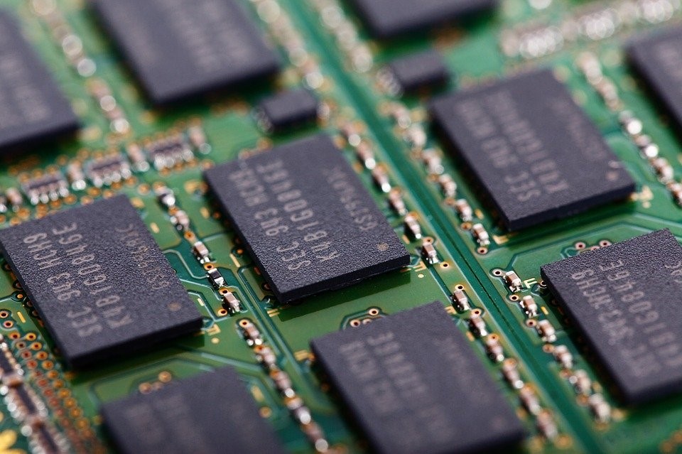
What is Flash Memory all about?
If you ever felt like an alien, when the conversation at a party diverted to certain tech subjects, were above your reach, then now is the time to build up your knowledge base. Flash memory is one such term, which is used in a number of components that are part of our day to day lives. The most common technique of storing modern day’s storage information is through Flash Memory. So, they are chances that, you already use it on daily or hourly basis, but little did you know about its importance in the computing world.
Flash Memory is known as a Non-Volatile memory, where the term “Non-Volatile” means, retaining the memory of a device, whether or not the device is electrically powered. It gained its name as such, due to the fact that the memory cells section is erased at the blink of the eye.
An example of a non-volatile memory is a hard disk, which retains all the data, even when the computer is turned off. However, flash memory has significant differences from hard disks. Both can retain data, even if the power is switched off. But flash memory differs in size, weight, and working function of a hard drive.
If you happen to use any kind of digital components that are compatible with the PC, then you probably own flash memory. Digital cameras, camcorders, video games and even GPS units utilize flash memory, in order to capture the related information, which can be later downloaded onto you PC.
Flash memory is available on different forms such as memory cards, memory sticks, USB drives and so on…. But the basic operating principle is same. The flash memory is simply versatile as it costs very little and is offered with the operating flexibility of simple plug and play option. The best part is that, the memory stored on this storage media, can be erased and re-written again.
How Flash Memory Works
It is a known fact that Flash memory is programmable and re-programmable. Flash Memory stores all the data in an array of cells made of Floating Gate Transistors. A Floating Gate Transistor is a Field Effect Transistor FET ( a FET is a transistor influenced by electric field, which is used to control the shape and the conductivity of a Channel of a particular charge carrier in a semiconductor material) which has identical structure to a conventional MOSFET. The gate of the FGMOS is electrically isolated and hence creates a floating node in the DC and a number of secondary gates or inputs are deposited above the FG and are also electrically insulated from it.
Historically, single level cell devices were used to store only one bit of information. But the new generation flash memory stores more than one bit per cell by choosing between multiple levels of electrical charge to apply to the floating gates of its cells. So for that reason, it is also known with names Multi level cell devices and triple level cell devices.
The term “Floating gate transistors” needs an explanation of flash memory. Each memory cell resembles a standard MOSFET (Metal oxide semiconductor field effect transistor). A MOSFET is a transistor used for amplifying or switching electronic signals. The difference is that the Floating Gate Transistor has two gates instead of one. On the top is the control gate or CG which is also seen in other MOS transistors. Below the CG is the floating gate which is FG and it is insulated around by an oxide layer.
The Floating gate is inter-imposed in-between the MOSFET channel and the control gate. As the Floating gate is insulated, the electrons placed in it, will not discharge for many years, under normal conditions. So, as a result, the FG holds the charge and isolates the CG from the electric field, which will modify the threshold voltage of the cell.
For a read-out, a voltage intermediate between the possible threshold voltages is applied to the Control Gate, and the Metal Oxide Semiconductor Field Effect Transistor channels conductivity is tested if it is conducting or insulating, which is influenced by the Floating gate. The current flow through the MOSFET channel is sensed and forms a binary code, which provides the stored data. The amount of current is sensed; in a multi level cell device which stores more than one bit per cell and this determines the level of charge on FG in a more precise way.
Flash memory works as a Basic Input Output System, known as BIOS in a PC. When the BIOS needs to be changed i.e. re-written, the flash memory writes in blocks, rather than bytes and so, offers a fast update. At the same time, Flash Memory is not practical to volatile RAM memory as Random access memory needs to be addressed at the byte level, rather than block level.
Flash Memory Types
They are two types of Flash Memory called NAND Memory & NOR Memory, where NAND allows to be programmed and is read in blocks and NOR allows to be written or read as byte.
NOR and NAND differ in two ways, where the connections of the individual memory cells are variant and the interface provided to read/write is also different.
NOR Flash – In a NOR gate, each individual cell has a direct connection of its one end to the ground, and the other end to the bit line. Since, this arrangement acts as a NOR gate( a combination of OR Gate followed by an inverter, which gives an output as TRUE if both inputs are false, or else the output is False), it is called as NOR flash, which can be explained as-When a single word lines, which is connected to the control gate or CG is carried high, its corresponding storage transistor puts the output bit line low. So, the low read latencies feature makes the NOR flash driven devices facilitate for both direct code execution and data storage in a single memory product. As a result, the NOR flash persists to be the technology of selection for embedded applications entailing a discrete non-volatile memory device.
Programming the NOR – A NOR flash cell at a single level is logically equivalent to a binary 1 value in a default state. This occurs due to the current flow through the channel under application of an appropriate voltage to the control gate. A NOR flash cell can be programmed in such a way, that it can be set to binary digit 0 value by following procedure-
- An elevated on-voltage, which is typically >5v is applied to CG.
- Channel is turned on, in order to make the electrons flow from the source to the drain.
- The source-drain current is sufficiently high to cause some high energy electrons to invade through the insulation layer onto the FG; by means of the process called as Hot-Electron injection (It is a phenomenon, where the electron achieves kinetic energy to overcome a potential barrier in order to break an interface state. The term HOT refers to the effective temperature used to model carrier density and it is not the overall temperature of the device.)
Erasing – in order to erase the NOR cell, or resetting it to the “1” state, a large voltage will be applied, which will be of opposite polarity. The application of voltage will be between CG and the source terminal, which will drag the electrons off the floating gate through the quantum tunneling, where a particle tunnels through a barrier with due force. The programming of NOR cells is generally performed one byte at a time. The erasing operation is only possible, when all the cells in a segment are erased at once. That is, the operations can be performed on a block wide basis.
NAND Flash – NAND flash also utilizes Floating Gate Transistors, but they are connected in a way that replicates NAND gate where several transistors are connected in series and only in case all word lines are pulled high, the bit line is pulled low. The NAND flash transistors group is connected to a NOR style bit line array in the same way that single transistors are linked in NOR flash. An extra level of addressing is seen in NAND, as replacing single transistors with serial linked groups is done. Bit level addressing will enable a single bit at a time access. But every bit in the word must be simultaneously addressed in order to execute in-place applications.
Reading – To read, the first desired group is selected. As a next thing most of the word lines are pulled up above the threshold voltage of a programmed bit in such a way that the pull up is just over the Threshold voltage of an erased bit. In case if the selected bit is not been programmed, the series group will conduct i.e. pull up the bit line low. Additional transistors presence will surely reduce the ground wires and bit lines presence, which will allow denser layout and greater storage capacity per chip. Traditionally, a NAND flash is permitted to contain a certain number of faults. Nowadays, manufactures are reducing the size of transistors in such a way that they are made reliable, by maximizing the amount of usable storage. However, the size must be further reduced in Transistor size which may increase the number of faults faster than, they would increase the available overall storage size.
Writing and erasing – NAND flash uses the tunnel injection for writing and tunnel release for erasing.
Advantages of Flash Memory
- It is a known fact that, Flash memory doesn’t rely on any electrically driven moving parts, which its other storage media siblings like hard disks, CDs, legacy old floppy disks and tapes rely on. The flash memory is independent of any mechanical means for storing and retrieving the data. Moving parts break down, damage, fail and become worn out and should be replaced on a regular front or should be maintained carefully. If the failure takes place in a vital moment, then data loss or delays in retrieving or storing of data can be observed. So, Flash memory has no moving parts and hence is durable and reliable.
- Normally, flash memory is available in different forms factors such as memory cards. These flash memory cards are available in different capacity ranges and volumes ranging till double digit Gigabit configuration (64GB).
- The highlighted benefit of Flash memory is that it offers faster read/write capabilities than hard disks.
- A Memory card, which is a form of flash memory, is so petite, that it is almost in the size of a coin and weighs the same. It can be carried anywhere and everywhere.
- Flash memory supports easy access to vital applications and so, the user can store a high end anti-malware program or a web browser in the flash drive (a form of flash memory) and can install them on a computer.
- Nowadays, flash memory drives are used in windows OSes like Windows 7 and Windows Vista, in order to increase the performance of the System.
- When the flash memory cards are used in high end video cameras, they simplify the management of storage and editing.


